What is the Process to Make a PCB

In today’s fast-paced technological landscape, understanding the intricacies of manufacturing processes like PCBs (Printed Circuit Boards) and PCBA (Printed Circuit Board Assembly) is essential. These components serve as the foundation for almost all electronic devices, from smartphones to industrial machinery. In this comprehensive guide, we’ll explore the step-by-step process of manufacturing PCBs, delve into the differences between PCBs and PCBA, and discuss the advantages and disadvantages of each.
Contents
Introduction to PCB Manufacturing Process
The PCB manufacturing process is a multi-step procedure that transforms raw materials into functional circuit boards. It’s a combination of engineering design, material science, and manufacturing expertise. Each stage of the process is critical in ensuring the final product meets the required specifications and quality standards.
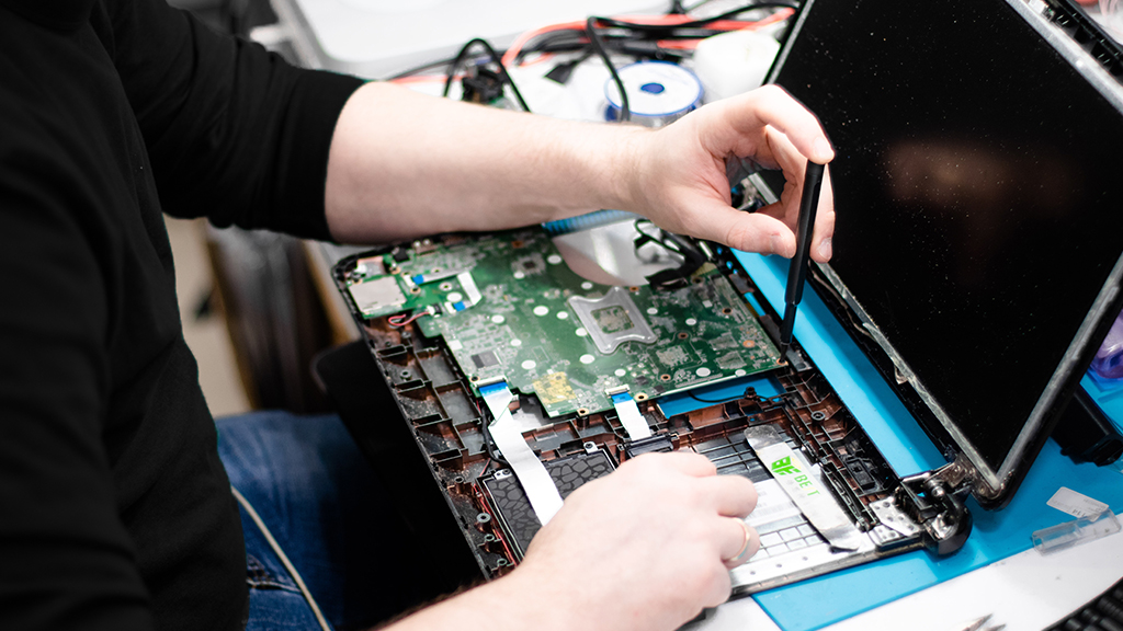
Understanding the differences between Printed Circuit Boards (PCBs) and Printed Circuit Board Assemblies (PCBAs) is paramount. A PCB serves as the backbone of electronic circuits, providing the foundation for electrical connections. Conversely, a PCB vs PCBA is a populated PCB, incorporating electronic components like resistors and capacitors. While PCBs are fundamental for prototyping, PCBA assemblies streamline mass production, enhancing device functionality. This comparison sheds light on their respective roles in the electronics manufacturing process.
Key Components and Materials Used in PCB Manufacturing
Substrates: The substrate, often made of fiberglass-reinforced epoxy resin (FR-4), provides the base for the PCB. It offers mechanical support and insulation for the conductive traces.
Copper Cladding: Copper foil is laminated onto the substrate to create conductive pathways for electrical signals. The thickness and quality of the copper layer significantly impact the performance and reliability of the PCB.
Solder Mask: A solder mask is applied over the copper traces to protect them from oxidation, corrosion, and solder bridging during assembly. It also enhances the durability of the PCB and facilitates component placement.
Silkscreen: The silkscreen layer is used to print component designators, logos, and other markings onto the PCB surface. It aids in component identification, assembly, and troubleshooting.
PCB Design
Schematic Design: The design process begins with creating a schematic diagram, outlining the electrical connections between components. This serves as a blueprint for the PCB layout.
PCB Layout: Using specialized design software, the PCB layout is created, specifying the placement of components and routing of traces. Factors such as signal integrity, thermal management, and manufacturability are considered during this phase.
PCB Fabrication Process
Preparing the Substrate: The substrate is cleaned and prepped for the fabrication process. Surface treatments may be applied to enhance adhesion and facilitate soldering.
Applying Copper Layers: Copper foil is bonded to both sides of the substrate using heat and pressure. The thickness of the copper layer is determined by the desired electrical properties of the PCB.
Etching: A chemical etching process is used to remove unwanted copper from the substrate, leaving behind the desired circuit traces. Precision and accuracy are crucial to ensure the integrity of the circuit pattern.
Drilling: Precision drilling machines are used to create holes for through-hole components and vias. The position and size of the holes are specified in the PCB design files.
Advantages and Disadvantages of PCB and PCBA
Advantages
- PCBA reduces the risk of assembly errors and improves the overall reliability of electronic devices.
- PCBA allows for automation in the assembly process, leading to increased production efficiency and scalability.
- PCBs and PCBA assemblies can be customized to meet specific design requirements and performance criteria.
Disadvantages
- PCBs require additional assembly steps and components, increasing production costs compared to simple electronic circuits.
- PCBA assemblies may be more susceptible to damage during handling and transportation due to the presence of delicate electronic components.
- Complex PCBA designs may pose challenges in terms of thermal management, signal integrity, and electromagnetic compatibility (EMC).
Conclusion
The process of making a PCB and PCBA involves a blend of design innovation, material science, and manufacturing expertise. From the initial schematic design to the final assembly and testing, each step plays a crucial role in producing high-quality electronic components that power our modern world. By understanding the intricacies of the PCB and PCBA manufacturing process, manufacturers can optimize production efficiency, enhance product reliability, and meet the evolving demands of the electronics industry.


